


One of the coolest things about getting into electronics and becoming a hacker is understanding how all the components in your hardware really work. Printed circuit boards (PCB) are used in almost all modern day electronics that you can think of without a doubt. From your computer’s motherboard, to some of the simplest single-board computers like the Arduino, we use them in one way or another. This guide at PCB manufacturers will answer all of your questions and teach you everything there is to know about them no matter how much or how little experience you have.
Table of Contents
What is actually a Printed Circuit Board?
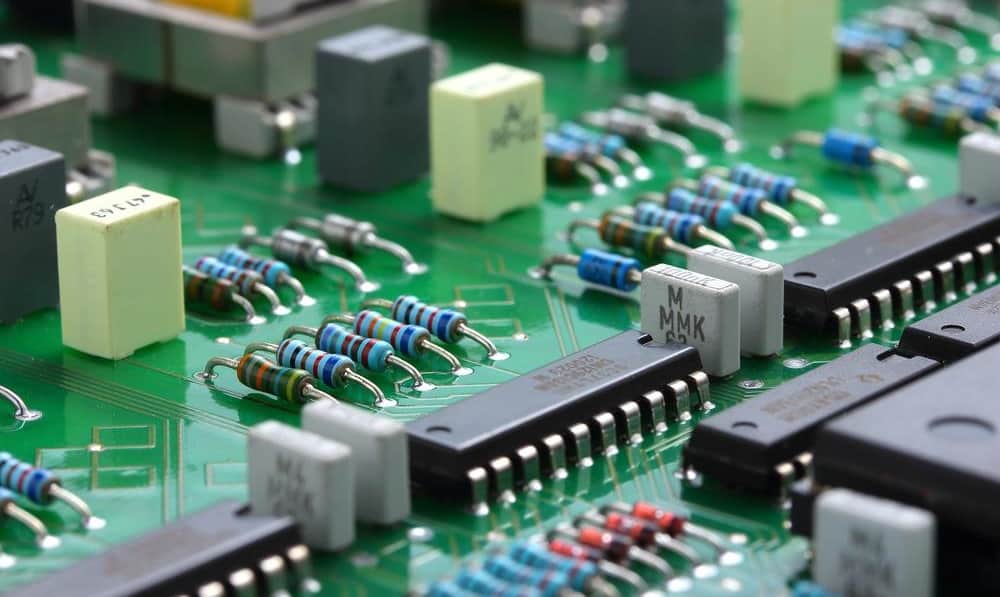
A printed circuit board is a flat surface with copper tracks embedded in it custom deck builder here. These tracks allow electricity to flow through the board and connect different electronic components together, like resistors or capacitors. The copper traces on the surface of the board are called traces, pads, or lands.
PCBs come in many different sizes and shapes depending on what they’re being used for: some might be very small while others can be quite large (like those found on calculators).
Some types of PCBs use layers of plastic instead of just one layer of metal traces; this is called multilayer or multilayer stackup construction (MLSC). Multi-layer construction allows manufacturers to add components on top of each other without having to worry about soldering them directly onto other
How does it work?
A PCB consists of a base layer made of copper and a top layer that serves as the “ground” for the circuit. The two layers are separated by an insulating material like fiberglass, which allows electricity to flow between them but keeps them from touching each other.
The way these boards work is pretty simple: electricity flows through the copper tracks, which are connected to each other by tiny metal pads called “pins.” These pins connect to components like resistors and capacitors, which help regulate the flow of electricity through the board itself.
The process of creating a PCB involves two steps: designing it and manufacturing it. The first step involves laying out all of the parts (like resistors and capacitors) on paper, then marking where they’ll go on your PCB by hand or with computer software. The second step is printing off freshly-made boards with your design already etched into them!
Why choose them?
Printed circuit boards (PCBs) are essential to the development of electronic devices. PCBs are most commonly used in industrial, commercial, and military applications. They have been around for over 30 years and have changed the world of electronics forever.
There are many reasons why you should choose printed circuit boards assembly service:
- Cost-effective – Printed circuit boards assembly services help you save money by reducing labor costs associated with manual assembly processes.
- Time-saving – PCB assembly services can be completed in a fraction of the time that it would take you to create your own PCBs at home or in a small workshop setting.
- Flexibility – These services allow you to experiment with various shapes, sizes, and materials without having to worry about building your own machinery or purchasing expensive equipment that might not work well with your needs (such as small batch production).
If you want your product to work properly but don’t have time or resources to create your own printed circuit boards, there’s no need to worry! You can hire our company to assemble them for you at a low cost. Our experts understand all aspects of PCB assembly service; from sourcing components from suppliers all around the world to assembling them into functional circuits that will fit seamlessly into your design plans.
Things to know before starting the PCB design:
1. PCB size — this depends on your product size (or enclosure size). Product size is defined during electronic engineering design process. You can see our video about it here.
2. PCB layers — the more layers, the more complex the manufacturing of the PCB will be. (Note: even a single layer PCB can be a complex one, but here we are talking about complexity to manufacture the PCBs. The more layers the PCB has, the more costly it will be to manufacture it).
- 2 layers usually for simple toy products
- 4 layers usually for IoT related products
- 6 to 8 layers usually for Smart phone or smart watch.
3. Your PCB manufacturer requirements. Make sure you read the guidelines about pacing, traces size, power isolation, and file naming before you start designing.
Information you will need to provide to the PCB manufacturer:
- Number of Layers (ex. 2, 4, 6,…etc.)
- Material (FR-2 (phenolic cotton paper), FR-3 (cotton paper and epoxy), FR-4 (woven glass and epoxy…etc.)
- Thickness (0.5 mm, 1.0 mm…etc.)
- Color (Red, Black, Green…etc.)
- Surface Finish (ENIG (Electroless Nickel/Immersion Gold), DIG (Direct Immersion Gold), OSP (Organic Solderability Preservatives…etc.)
- Copper Weight (1 oz (35 um), 2 oz (70 um), 0.5 oz (18 um)…etc.)
- Gerber file
PCB design process:
Circuit Design
For this step you need to create a schematic. It is a document, like a blueprint, that describes how components relate to each other and work together. To create a schematic file, you will need a software tool. We like Quadcept, as it is optimized for designing PCBs for manufacturing (for example, you can export your Bill of Materials (BoM) directly from the tool) and, being cloud-based, it can be conveniently used anywhere. (They also have a free Community Version of the tool for makers and students).
There are also many others you can choose from:
- Altium
- ExpressPCB
- Upverter
- KiCad
- Cadence Allegro
- PADs
- ORCAD
- DipTrace
After you have the selected tool installed, you need to get component specifications for each of your selected components. They are usually available on your vendors’ websites. The model files will help you to draw the schematic. When you upload the model to the software tool, the component will be available in the database. Then all you need to do is to follow the data sheet to connect the lines to each pin out of the components. (Note: specifics of the design process will depend on the software tool of choice).
Each schematic symbol needs to have an associated PCB footprint that defines the physical dimensions of the components, and placement of the copper pads or through-holes on the PCB. You should already have your components selected (or select them now), and we covered this procedure in the EE design flow video